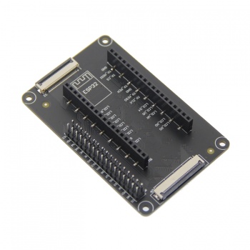
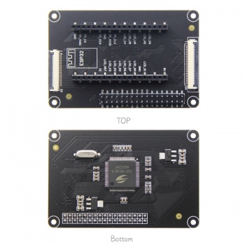
Difference between revisions of "SSD1963-RGB Pinboard"
(→产品图片) |
(→Packing List) |
||
| (17 intermediate revisions by 2 users not shown) | |||
| Line 1: | Line 1: | ||
{{lan | {{lan | ||
| | | | ||
| − | cn=http://www.lcdwiki.com/zh/SSD1963- | + | cn=http://www.lcdwiki.com/zh/SSD1963-RGB_Pinboard |
| | | | ||
en=http://www.lcdwiki.com/SSD1963-RGB_Pinboard | en=http://www.lcdwiki.com/SSD1963-RGB_Pinboard | ||
}} | }} | ||
| − | ==<font color="blue"> | + | ==<font color="blue">Product Picture</font> == |
[[File:RGB转接板-3.jpg|350px]] | [[File:RGB转接板-3.jpg|350px]] | ||
[[File:RGB转接板-2pin.jpg|350px]] | [[File:RGB转接板-2pin.jpg|350px]] | ||
| − | ==<font color="blue"> | + | ==<font color="blue">Product Description</font> == |
| + | * The ssd1963 control IC is On board | ||
| + | * Support the highest resolution of 800*480 | ||
| + | * Support the direct connection of flexible cable and needle of STM32 development board | ||
| + | * Support direct insertion of esp32 development board | ||
| + | * Support direct connection of RGB display module flexible cable | ||
| + | * Support 8-bit and 16 bit parallel bus transmission, transmission speed block | ||
| + | * Provide rich STM32 platform and esp32 platform sample program | ||
| + | * Military grade process standard, long-term stable work | ||
| + | * Provide technical support for underlying driver | ||
| + | ==<font color="blue">Product Parameters</font> == | ||
| + | {| class="wikitable" border="1" style="width: 500px; background-color: white;" | ||
| + | | align="center" |Name | ||
| + | | align="center" |Parameter | ||
| + | |- | ||
| + | | align="center" |SKU | ||
| + | | align="center" |SSD1963 | ||
| + | |- | ||
| + | | align="center" |Driver IC | ||
| + | | align="center" |SSD1963 | ||
| + | |- | ||
| + | | align="center" |Highest Resolution | ||
| + | | align="center" |800*480 | ||
| + | |- | ||
| + | | align="center" |STM32 development board input interface | ||
| + | | align="center" |16 bit parallel port | ||
| + | |- | ||
| + | | align="center" |Input interface of esp32 development board | ||
| + | | align="center" |8 bit parallel port | ||
| + | |- | ||
| + | | align="center" |Output interface | ||
| + | | align="center" |24 bit RGB parallel port | ||
| + | |- | ||
| + | | align="center" |Module PCB Size | ||
| + | | align="center" |50.00x77.00(mm) | ||
| + | |- | ||
| + | | align="center" |Input Voltage | ||
| + | | align="center" |5V | ||
| + | |- | ||
| + | | align="center" |IO Voltage | ||
| + | | align="center" |3.3V and 1.8V | ||
| + | |- | ||
| + | | align="center" |Power Consumption | ||
| + | | align="center" |36mA | ||
| + | |- | ||
| + | | align="center" |Rough Weight(Net weight) | ||
| + | | align="center" |22 (g) | ||
| + | |} | ||
| − | ==<font color="blue"> | + | ==<font color="blue">Interface Definition</font> == |
| + | [[File:SSD1963-001.png|650px]] | ||
| − | + | :①--40pin flexible cable output interface | |
| − | + | :②④--In line interface of esp32 development board | |
| + | :③--STM32 development board 32pin flexible cable input interface | ||
| + | :⑤--STM32 development board 34pin pin input interface | ||
| − | ==<font color="blue"> | + | *'''STM32 development board row pin input interface pin description''' |
| + | |||
| + | {| class="wikitable" border="1" style="width: 600px; background-color: white;" | ||
| + | |- | ||
| + | | align="center" |Number | ||
| + | | align="center" |Pin name | ||
| + | | align="center" |Description | ||
| + | |- | ||
| + | | align="center" |1 | ||
| + | | align="center" |CS | ||
| + | |LCD reset control pin( low level enable) | ||
| + | |- | ||
| + | | align="center" |2 | ||
| + | | align="center" |RS | ||
| + | |LCD register / data selection control pin(high level: register, low level: data) | ||
| + | |- | ||
| + | | align="center" |3 | ||
| + | | align="center" |WR | ||
| + | |LCD write control pin | ||
| + | |- | ||
| + | | align="center" |4 | ||
| + | | align="center" |RD | ||
| + | |LCD read control pin | ||
| + | |- | ||
| + | | align="center" |5 | ||
| + | | align="center" |RST | ||
| + | |LCD reset control pin( low level reset) | ||
| + | |- | ||
| + | | align="center" |6~21 | ||
| + | | align="center" |D0~D15 | ||
| + | |LCD 16 bit data bus pin (use d0 ~ D7 in 8-bit mode) | ||
| + | |- | ||
| + | | align="center" |22 | ||
| + | | align="center" |GND | ||
| + | |Module power ground pin | ||
| + | |- | ||
| + | | align="center" |23 | ||
| + | | align="center" |TE | ||
| + | |LCD tearing effect signal pin (read only) | ||
| + | |- | ||
| + | | align="center" |24 | ||
| + | | align="center" |NC | ||
| + | |No definition, reserved | ||
| + | |- | ||
| + | | align="center" |25 | ||
| + | | align="center" |NC | ||
| + | |No definition, reserved | ||
| + | |- | ||
| + | | align="center" |26 | ||
| + | | align="center" |GND | ||
| + | |Module power ground pin | ||
| + | |- | ||
| + | | align="center" |27 | ||
| + | | align="center" |GND | ||
| + | |Module power ground pin | ||
| + | |- | ||
| + | | align="center" |28 | ||
| + | | align="center" |5V | ||
| + | |Module power supply positive pin (connected to 5V) | ||
| + | |- | ||
| + | | align="center" |29 | ||
| + | | align="center" |TMI | ||
| + | |Resistance touch screen SPI bus read data pin (capacitor touch screen not used) | ||
| + | |- | ||
| + | | align="center" |30 | ||
| + | | align="center" |TMO | ||
| + | |IIC bus data pin of capacitive touch screen (SPI bus write data pin of resistance touch screen) | ||
| + | |- | ||
| + | | align="center" |31 | ||
| + | | align="center" |PEN | ||
| + | |Touch screen interrupt detection pin(Low level when a touch occurs) | ||
| + | |- | ||
| + | | align="center" |32 | ||
| + | | align="center" |NC | ||
| + | |No definition, reserved | ||
| + | |- | ||
| + | | align="center" |33 | ||
| + | | align="center" |TCS | ||
| + | |Capacitor touch screen reset pin (resistance touch screen chip selection pin) | ||
| + | |- | ||
| + | | align="center" |34 | ||
| + | | align="center" |TCK | ||
| + | |IIC bus clock pin of capacitive touch screen (SPI bus clock pin of resistance touch screen) | ||
| + | |- | ||
| + | |} | ||
| + | |||
| + | *'''STM32 development board flexible cable input interface pin description''' | ||
| + | |||
| + | {| class="wikitable" border="1" style="width: 600px; background-color: white;" | ||
| + | |- | ||
| + | | align="center" |Number | ||
| + | | align="center" |Pin name | ||
| + | | align="center" |Description | ||
| + | |- | ||
| + | | align="center" |1 | ||
| + | | align="center" |TCK | ||
| + | |IIC bus clock pin of capacitive touch screen (SPI bus clock pin of resistance touch screen) | ||
| + | |- | ||
| + | | align="center" |2 | ||
| + | | align="center" |TCS | ||
| + | |Capacitor touch screen reset pin (resistance touch screen chip selection pin) | ||
| + | |- | ||
| + | | align="center" |3 | ||
| + | | align="center" |PEN | ||
| + | |Touch screen interrupt detection pin(Low level when a touch occurs) | ||
| + | |- | ||
| + | | align="center" |4 | ||
| + | | align="center" |TMO | ||
| + | |IIC bus data pin of capacitive touch screen (SPI bus write data pin of resistance touch screen) | ||
| + | |- | ||
| + | | align="center" |5 | ||
| + | | align="center" |TMI | ||
| + | |Resistance touch screen SPI bus read data pin (capacitor touch screen not used) | ||
| + | |- | ||
| + | | align="center" |6 | ||
| + | | align="center" |5V | ||
| + | |Module power supply positive pin (connected to 5V) | ||
| + | |- | ||
| + | | align="center" |7 | ||
| + | | align="center" |GND | ||
| + | |Module power ground pin | ||
| + | |- | ||
| + | | align="center" |8 | ||
| + | | align="center" |GND | ||
| + | |Module power ground pin | ||
| + | |- | ||
| + | | align="center" |9 | ||
| + | | align="center" |NC | ||
| + | |No definition, reserved | ||
| + | |- | ||
| + | | align="center" |10 | ||
| + | | align="center" |NC | ||
| + | |No definition, reserved | ||
| + | |- | ||
| + | | align="center" |11 | ||
| + | | align="center" |TE | ||
| + | |LCD tearing effect signal pin (read only) | ||
| + | |- | ||
| + | | align="center" |12~27 | ||
| + | | align="center" |D15~D0 | ||
| + | |LCD 16 bit data bus pin (use d0 ~ D7 in 8-bit mode) | ||
| + | |- | ||
| + | | align="center" |28 | ||
| + | | align="center" |RST | ||
| + | |LCD reset control pin( low level reset) | ||
| + | |- | ||
| + | | align="center" |29 | ||
| + | | align="center" |RD | ||
| + | |LCD read control pin | ||
| + | |- | ||
| + | | align="center" |30 | ||
| + | | align="center" |WR | ||
| + | |LCD write control pin | ||
| + | |- | ||
| + | | align="center" |31 | ||
| + | | align="center" |RS | ||
| + | |LCD register / data selection control pin(high level: register, low level: data) | ||
| + | |- | ||
| + | | align="center" |32 | ||
| + | | align="center" |CS | ||
| + | |LCD reset control pin( low level enable) | ||
| + | |- | ||
| + | |} | ||
| + | |||
| + | *'''ESP32 development board''' '''in line interface pin description''' | ||
| + | |||
| + | {| class="wikitable" border="1" style="width: 600px; background-color: white;" | ||
| + | |- | ||
| + | | align="center" |Number | ||
| + | | align="center" |Pin name | ||
| + | | align="center" |Description | ||
| + | |- | ||
| + | | align="center" |1 | ||
| + | | align="center" |5V | ||
| + | |power pin (connected to 5V) | ||
| + | |- | ||
| + | | align="center" |2 | ||
| + | | align="center" |LCD_RS | ||
| + | |LCD register / data selection control pin(high level: register, low level: data) | ||
| + | |- | ||
| + | | align="center" |3 | ||
| + | | align="center" |LCD_RD | ||
| + | |LCD read control pin | ||
| + | |- | ||
| + | | align="center" |4 | ||
| + | | align="center" |LCD_D1 | ||
| + | |Pin 2 of 8-bit parallel data bus | ||
| + | |- | ||
| + | | align="center" |5 | ||
| + | | align="center" |GND | ||
| + | |Power ground pin | ||
| + | |- | ||
| + | | align="center" |6 | ||
| + | | align="center" |LCD_WR | ||
| + | |LCD write control pin | ||
| + | |- | ||
| + | | align="center" |7 | ||
| + | | align="center" |LCD_D0 | ||
| + | |Pin 1 of 8-bit parallel data bus | ||
| + | |- | ||
| + | | align="center" |8 | ||
| + | | align="center" |LCD_D5 | ||
| + | |Pin 6 of 8-bit parallel data bus | ||
| + | |- | ||
| + | | align="center" |9 | ||
| + | | align="center" |LCD_D7 | ||
| + | |Pin 8 of 8-bit parallel data bus | ||
| + | |- | ||
| + | | align="center" |10 | ||
| + | | align="center" |LCD_D4 | ||
| + | |Pin 5 of 8-bit parallel data bus | ||
| + | |- | ||
| + | | align="center" |11 | ||
| + | | align="center" |LCD_D6 | ||
| + | |Pin 7 of 8-bit parallel data bus | ||
| + | |- | ||
| + | | align="center" |12 | ||
| + | | align="center" |LCD_D2 | ||
| + | |Pin 3 of 8-bit parallel data bus | ||
| + | |- | ||
| + | | align="center" |13 | ||
| + | | align="center" |TP_CLK | ||
| + | |IIC bus clock control pin of capacitive touch screen(SPI bus clock control pin of resistance touch screen) | ||
| + | |- | ||
| + | | align="center" |14 | ||
| + | | align="center" |LCD_D3 | ||
| + | |Pin 4 of 8-bit parallel data bus | ||
| + | |- | ||
| + | | align="center" |15 | ||
| + | | align="center" |TP_MISO | ||
| + | |SPI bus read data pin of resistance touch screen(capacitive touch screen not used) | ||
| + | |- | ||
| + | | align="center" |16 | ||
| + | | align="center" |LCD_CS | ||
| + | |LCD chip select control pin | ||
| + | |- | ||
| + | | align="center" |17 | ||
| + | | align="center" |GND | ||
| + | |Power ground pin | ||
| + | |- | ||
| + | | align="center" |18 | ||
| + | | align="center" |LCD_RST | ||
| + | |LCD reset control pin | ||
| + | |- | ||
| + | | align="center" |19 | ||
| + | | align="center" |TP_PEN | ||
| + | |Touch screen interrupt control pin | ||
| + | |- | ||
| + | | align="center" |20 | ||
| + | | align="center" |TE | ||
| + | |Tearing Effect Signal pin(read-only) | ||
| + | |- | ||
| + | | align="center" |21 | ||
| + | | align="center" |TP_CS | ||
| + | |Capacitive touch screen reset pin(resistance touch screen chip selection pin) | ||
| + | |- | ||
| + | | align="center" |22 | ||
| + | | align="center" |TP_MOSI | ||
| + | |IIC bus data pin of capacitive touch screen(resistance touch screen SPI bus write data pin) | ||
| + | |- | ||
| + | | align="center" |23 | ||
| + | | align="center" |GND | ||
| + | |Power ground pin | ||
| + | |- | ||
| + | |} | ||
| + | |||
| + | *'''Pin description of flexible cable output interface''' | ||
| + | |||
| + | {| class="wikitable" border="1" style="width: 600px; background-color: white;" | ||
| + | |- | ||
| + | | align="center" |Number | ||
| + | | align="center" |Pin name | ||
| + | | align="center" |Description | ||
| + | |- | ||
| + | | align="center" |1 | ||
| + | | align="center" |VCC5 | ||
| + | |Power input pin(connect to 5V) | ||
| + | |- | ||
| + | | align="center" |2 | ||
| + | | align="center" |VCC5 | ||
| + | |Power input pin(connect to 5V) | ||
| + | |- | ||
| + | | align="center" |3~10 | ||
| + | | align="center" |R0~R7 | ||
| + | |8-bit RED data pin | ||
| + | |- | ||
| + | | align="center" |11 | ||
| + | | align="center" |GND | ||
| + | |power ground pin | ||
| + | |- | ||
| + | | align="center" |12~19 | ||
| + | | align="center" |G0 ~ G7 | ||
| + | |8-bit GREEN data pin | ||
| + | |- | ||
| + | | align="center" |20 | ||
| + | | align="center" |GND | ||
| + | |power ground pin | ||
| + | |- | ||
| + | | align="center" |21~28 | ||
| + | | align="center" |B0 ~ B7 | ||
| + | |8-bit GREEN data pin | ||
| + | |- | ||
| + | | align="center" |29 | ||
| + | | align="center" |GND | ||
| + | |power ground pin | ||
| + | |- | ||
| + | | align="center" |30 | ||
| + | | align="center" |PCLK | ||
| + | |Pixel clock control pin | ||
| + | |- | ||
| + | | align="center" |31 | ||
| + | | align="center" |HSYNC | ||
| + | |Horizontal synchronous signal control pin | ||
| + | |- | ||
| + | | align="center" |32 | ||
| + | | align="center" |VSYNC | ||
| + | |Vertical synchronous signal control pin | ||
| + | |- | ||
| + | | align="center" |33 | ||
| + | | align="center" |DE | ||
| + | |Data enable signal control pin | ||
| + | |- | ||
| + | | align="center" |34 | ||
| + | | align="center" |BL | ||
| + | |LCD backlight control pin | ||
| + | |- | ||
| + | | align="center" |35 | ||
| + | | align="center" |TP_CS | ||
| + | |Capacitor touch screen reset pin (resistance touch screen chip selection pin) | ||
| + | |- | ||
| + | | align="center" |36 | ||
| + | | align="center" |TP_MOSI | ||
| + | |Data pin of IIC bus of capacitance touch screen (write data pin of SPI bus of resistance touch screen) | ||
| + | |- | ||
| + | | align="center" |37 | ||
| + | | align="center" |TP_MISO | ||
| + | |Resistance touch screen SPI bus read data pin (capacitance touch screen not used) | ||
| + | |- | ||
| + | | align="center" |38 | ||
| + | | align="center" |TP_CLK | ||
| + | |IIC bus clock control pin of capacitive touch screen (SPI bus clock control pin of resistance touch screen) | ||
| + | |- | ||
| + | | align="center" |39 | ||
| + | | align="center" |TP_PEN | ||
| + | |Touch screen interrupt control pin (low level when touch is generated) | ||
| + | |- | ||
| + | | align="center" |40 | ||
| + | | align="center" |RST | ||
| + | |LCD reset control pin (effective at low level) | ||
| + | |- | ||
| + | |} | ||
| + | |||
| + | ==<font color="blue">How to Connect</font> == | ||
[[File:5-RGB-转接板-原子小系统板.jpg|750px]] | [[File:5-RGB-转接板-原子小系统板.jpg|750px]] | ||
[[File:5-RGB-转接板-STM32F407.jpg|750px]] | [[File:5-RGB-转接板-STM32F407.jpg|750px]] | ||
[[File:5-RGB-ESP32-2.jpg|750px]] | [[File:5-RGB-ESP32-2.jpg|750px]] | ||
| + | |||
| + | ==<font color="blue">Packing List</font> == | ||
| + | [[File:SSD1963-004.jpg|750px]] | ||
| + | |||
| + | ==<font color="blue">Program Download</font> == | ||
| + | * [http://www.lcdwiki.com/res/Program/RGB_LCD/4.3inch/MCU_Display_SSD1963_V1.0/4.3inch_MCU_Display_SSD1963_V1.0.zip '''4.3inch SSD1963 MCU Display Module package'''] | ||
| + | * [http://www.lcdwiki.com/res/Program/RGB_LCD/5.0inch/MCU_Display_SSD1963_V1.0/5.0inch_MCU_Display_SSD1963_V1.0.zip '''5.0inch SSD1963 MCU Display Module package'''] | ||
| + | * [http://www.lcdwiki.com/res/Program/RGB_LCD/7.0inch/MCU_Display_SSD1963_V1.0/7.0inch_MCU_Display_SSD1963_V1.0.zip '''7.0inch SSD1963 MCU Display Module package'''] | ||
| + | |||
| + | ==<font color="blue">Product Documentation</font> == | ||
| + | * [http://www.lcdwiki.com/res/SSD1963/4.3inch_MCU_Display_SSD1963_User_Manual_EN.pdf '''4.3inch SSD1963 MCU Display Module User Manual'''] | ||
| + | * [http://www.lcdwiki.com/res/SSD1963/5.0inch_MCU_Display_SSD1963_User_Manual_EN.pdf '''5.0inch SSD1963 MCU Display Module User Manual'''] | ||
| + | * [http://www.lcdwiki.com/res/SSD1963/7.0inch_MCU_Display_SSD1963_User_Manual_EN.pdf '''7.0inch SSD1963 MCU Display Module User Manual'''] | ||
| + | * [http://www.lcdwiki.com/zh/images/0/0f/SSD1963-002.jpg '''SSD19963 Pinboard Size picture-front'''] | ||
| + | * [http://www.lcdwiki.com/zh/images/f/f6/SSD1963-003.jpg '''SSD19963 Pinboard Size picture-back'''] | ||
| + | * [http://www.lcdwiki.com/res/SSD1963/SSD1963_Board_Schematic.pdf '''SSD1963 Pinboard Schematic'''] | ||
| + | * [http://www.lcdwiki.com/res/SSD1963/SSD1963_DS_V1.1.pdf '''Driver IC SSD1963 Data sheet'''] | ||
| + | |||
| + | ==<font color="blue">Reference Materials</font> == | ||
| + | * [http://www.lcdwiki.com/res/PublicFile/STM32_Keil_Use_Illustration_EN.pdf '''STM32 keil software use illustration'''] | ||
| + | * [http://www.lcdwiki.com/res/PublicFile/Arduino_IDE_Use_Illustration_EN.pdf '''Arduino IDE software use illustration'''] | ||
| + | * [http://www.lcdwiki.com/res/PublicFile/Arduino_For_ESP32_Installation_Instructions_EN.pdf '''Arduino IDE For ESP32 Install Instructions'''] | ||
| + | * [http://www.lcdwiki.com/res/PublicFile/PCtoLCD2002_Use_Illustration_EN.pdf '''PCtoLCD2002 software use illustration'''] | ||
| + | * [http://www.lcdwiki.com/res/PublicFile/Image2Lcd_Use_Illustration_EN.pdf '''Image2Lcd software use illustration'''] | ||
| + | * [http://www.lcdwiki.com/Chinese_and_English_display_modulo_settings '''Chinese and English display modulo settings'''] | ||
| + | |||
| + | ==<font color="blue">Common Software</font> == | ||
| + | |||
| + | * [http://www.lcdwiki.com/res/software/PCtoLCD2002.zip '''PCtoLCD2002'''] | ||
| + | * [http://www.lcdwiki.com/res/software/Image2Lcd.zip '''Image2Lcd'''] | ||
Latest revision as of 16:29, 25 April 2021
Contents
Product Picture
Product Description
- The ssd1963 control IC is On board
- Support the highest resolution of 800*480
- Support the direct connection of flexible cable and needle of STM32 development board
- Support direct insertion of esp32 development board
- Support direct connection of RGB display module flexible cable
- Support 8-bit and 16 bit parallel bus transmission, transmission speed block
- Provide rich STM32 platform and esp32 platform sample program
- Military grade process standard, long-term stable work
- Provide technical support for underlying driver
Product Parameters
| Name | Parameter |
| SKU | SSD1963 |
| Driver IC | SSD1963 |
| Highest Resolution | 800*480 |
| STM32 development board input interface | 16 bit parallel port |
| Input interface of esp32 development board | 8 bit parallel port |
| Output interface | 24 bit RGB parallel port |
| Module PCB Size | 50.00x77.00(mm) |
| Input Voltage | 5V |
| IO Voltage | 3.3V and 1.8V |
| Power Consumption | 36mA |
| Rough Weight(Net weight) | 22 (g) |
Interface Definition
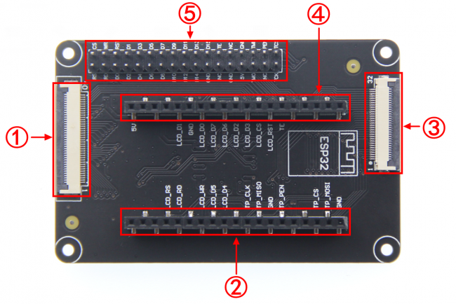
- ①--40pin flexible cable output interface
- ②④--In line interface of esp32 development board
- ③--STM32 development board 32pin flexible cable input interface
- ⑤--STM32 development board 34pin pin input interface
- STM32 development board row pin input interface pin description
| Number | Pin name | Description |
| 1 | CS | LCD reset control pin( low level enable) |
| 2 | RS | LCD register / data selection control pin(high level: register, low level: data) |
| 3 | WR | LCD write control pin |
| 4 | RD | LCD read control pin |
| 5 | RST | LCD reset control pin( low level reset) |
| 6~21 | D0~D15 | LCD 16 bit data bus pin (use d0 ~ D7 in 8-bit mode) |
| 22 | GND | Module power ground pin |
| 23 | TE | LCD tearing effect signal pin (read only) |
| 24 | NC | No definition, reserved |
| 25 | NC | No definition, reserved |
| 26 | GND | Module power ground pin |
| 27 | GND | Module power ground pin |
| 28 | 5V | Module power supply positive pin (connected to 5V) |
| 29 | TMI | Resistance touch screen SPI bus read data pin (capacitor touch screen not used) |
| 30 | TMO | IIC bus data pin of capacitive touch screen (SPI bus write data pin of resistance touch screen) |
| 31 | PEN | Touch screen interrupt detection pin(Low level when a touch occurs) |
| 32 | NC | No definition, reserved |
| 33 | TCS | Capacitor touch screen reset pin (resistance touch screen chip selection pin) |
| 34 | TCK | IIC bus clock pin of capacitive touch screen (SPI bus clock pin of resistance touch screen) |
- STM32 development board flexible cable input interface pin description
| Number | Pin name | Description |
| 1 | TCK | IIC bus clock pin of capacitive touch screen (SPI bus clock pin of resistance touch screen) |
| 2 | TCS | Capacitor touch screen reset pin (resistance touch screen chip selection pin) |
| 3 | PEN | Touch screen interrupt detection pin(Low level when a touch occurs) |
| 4 | TMO | IIC bus data pin of capacitive touch screen (SPI bus write data pin of resistance touch screen) |
| 5 | TMI | Resistance touch screen SPI bus read data pin (capacitor touch screen not used) |
| 6 | 5V | Module power supply positive pin (connected to 5V) |
| 7 | GND | Module power ground pin |
| 8 | GND | Module power ground pin |
| 9 | NC | No definition, reserved |
| 10 | NC | No definition, reserved |
| 11 | TE | LCD tearing effect signal pin (read only) |
| 12~27 | D15~D0 | LCD 16 bit data bus pin (use d0 ~ D7 in 8-bit mode) |
| 28 | RST | LCD reset control pin( low level reset) |
| 29 | RD | LCD read control pin |
| 30 | WR | LCD write control pin |
| 31 | RS | LCD register / data selection control pin(high level: register, low level: data) |
| 32 | CS | LCD reset control pin( low level enable) |
- ESP32 development board in line interface pin description
| Number | Pin name | Description |
| 1 | 5V | power pin (connected to 5V) |
| 2 | LCD_RS | LCD register / data selection control pin(high level: register, low level: data) |
| 3 | LCD_RD | LCD read control pin |
| 4 | LCD_D1 | Pin 2 of 8-bit parallel data bus |
| 5 | GND | Power ground pin |
| 6 | LCD_WR | LCD write control pin |
| 7 | LCD_D0 | Pin 1 of 8-bit parallel data bus |
| 8 | LCD_D5 | Pin 6 of 8-bit parallel data bus |
| 9 | LCD_D7 | Pin 8 of 8-bit parallel data bus |
| 10 | LCD_D4 | Pin 5 of 8-bit parallel data bus |
| 11 | LCD_D6 | Pin 7 of 8-bit parallel data bus |
| 12 | LCD_D2 | Pin 3 of 8-bit parallel data bus |
| 13 | TP_CLK | IIC bus clock control pin of capacitive touch screen(SPI bus clock control pin of resistance touch screen) |
| 14 | LCD_D3 | Pin 4 of 8-bit parallel data bus |
| 15 | TP_MISO | SPI bus read data pin of resistance touch screen(capacitive touch screen not used) |
| 16 | LCD_CS | LCD chip select control pin |
| 17 | GND | Power ground pin |
| 18 | LCD_RST | LCD reset control pin |
| 19 | TP_PEN | Touch screen interrupt control pin |
| 20 | TE | Tearing Effect Signal pin(read-only) |
| 21 | TP_CS | Capacitive touch screen reset pin(resistance touch screen chip selection pin) |
| 22 | TP_MOSI | IIC bus data pin of capacitive touch screen(resistance touch screen SPI bus write data pin) |
| 23 | GND | Power ground pin |
- Pin description of flexible cable output interface
| Number | Pin name | Description |
| 1 | VCC5 | Power input pin(connect to 5V) |
| 2 | VCC5 | Power input pin(connect to 5V) |
| 3~10 | R0~R7 | 8-bit RED data pin |
| 11 | GND | power ground pin |
| 12~19 | G0 ~ G7 | 8-bit GREEN data pin |
| 20 | GND | power ground pin |
| 21~28 | B0 ~ B7 | 8-bit GREEN data pin |
| 29 | GND | power ground pin |
| 30 | PCLK | Pixel clock control pin |
| 31 | HSYNC | Horizontal synchronous signal control pin |
| 32 | VSYNC | Vertical synchronous signal control pin |
| 33 | DE | Data enable signal control pin |
| 34 | BL | LCD backlight control pin |
| 35 | TP_CS | Capacitor touch screen reset pin (resistance touch screen chip selection pin) |
| 36 | TP_MOSI | Data pin of IIC bus of capacitance touch screen (write data pin of SPI bus of resistance touch screen) |
| 37 | TP_MISO | Resistance touch screen SPI bus read data pin (capacitance touch screen not used) |
| 38 | TP_CLK | IIC bus clock control pin of capacitive touch screen (SPI bus clock control pin of resistance touch screen) |
| 39 | TP_PEN | Touch screen interrupt control pin (low level when touch is generated) |
| 40 | RST | LCD reset control pin (effective at low level) |
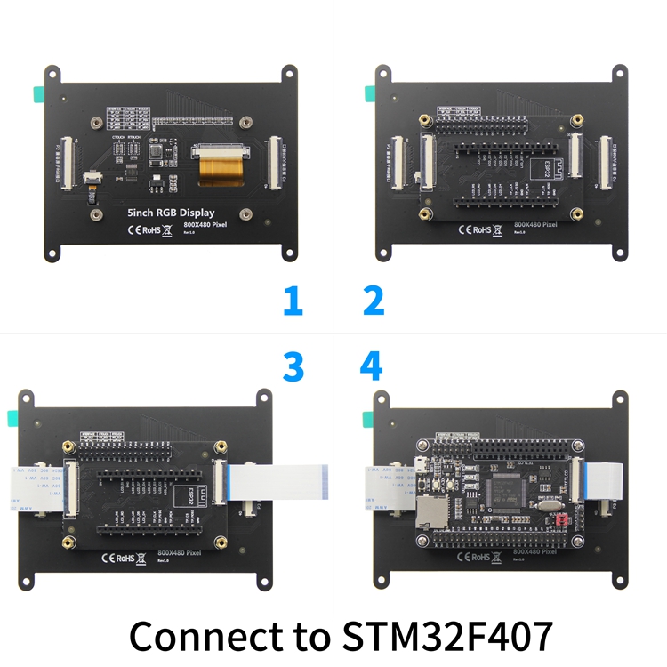
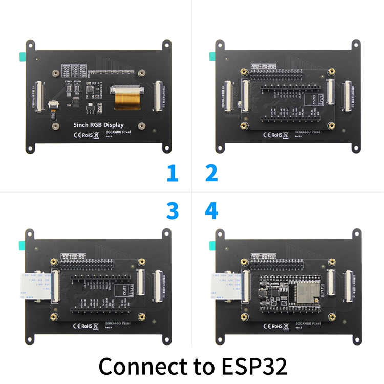
How to Connect
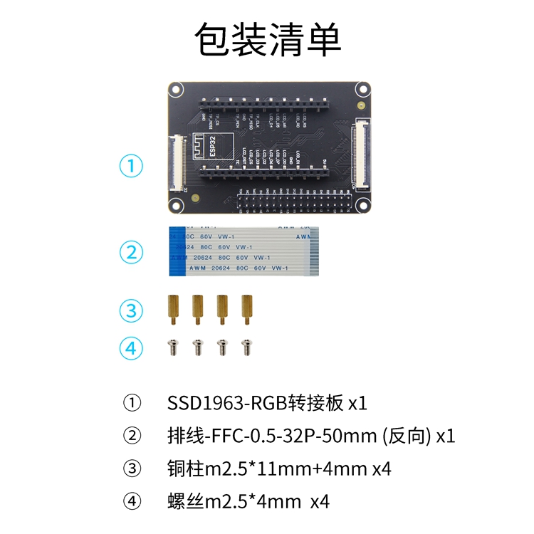
Packing List
Program Download
- 4.3inch SSD1963 MCU Display Module package
- 5.0inch SSD1963 MCU Display Module package
- 7.0inch SSD1963 MCU Display Module package
Product Documentation
- 4.3inch SSD1963 MCU Display Module User Manual
- 5.0inch SSD1963 MCU Display Module User Manual
- 7.0inch SSD1963 MCU Display Module User Manual
- SSD19963 Pinboard Size picture-front
- SSD19963 Pinboard Size picture-back
- SSD1963 Pinboard Schematic
- Driver IC SSD1963 Data sheet
Reference Materials
- STM32 keil software use illustration
- Arduino IDE software use illustration
- Arduino IDE For ESP32 Install Instructions
- PCtoLCD2002 software use illustration
- Image2Lcd software use illustration
- Chinese and English display modulo settings
