More actions
No edit summary |
|||
| Line 13: | Line 13: | ||
* The ssd1963 control IC is On board | * The ssd1963 control IC is On board | ||
* Support the highest resolution of 800*480 | |||
* Support the direct connection of flexible cable and needle of STM32 development board | * Support the direct connection of flexible cable and needle of STM32 development board | ||
* Support direct insertion of esp32 development board | * Support direct insertion of esp32 development board | ||
Revision as of 14:10, 15 March 2021
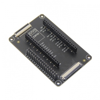
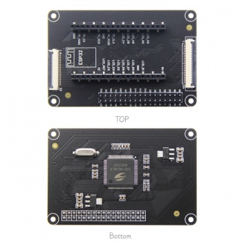
Product Picture
Product Description
- The ssd1963 control IC is On board
- Support the highest resolution of 800*480
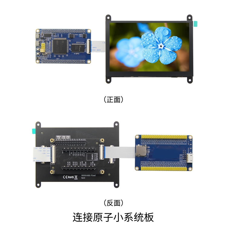
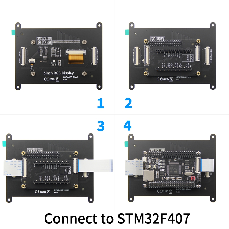
- Support the direct connection of flexible cable and needle of STM32 development board
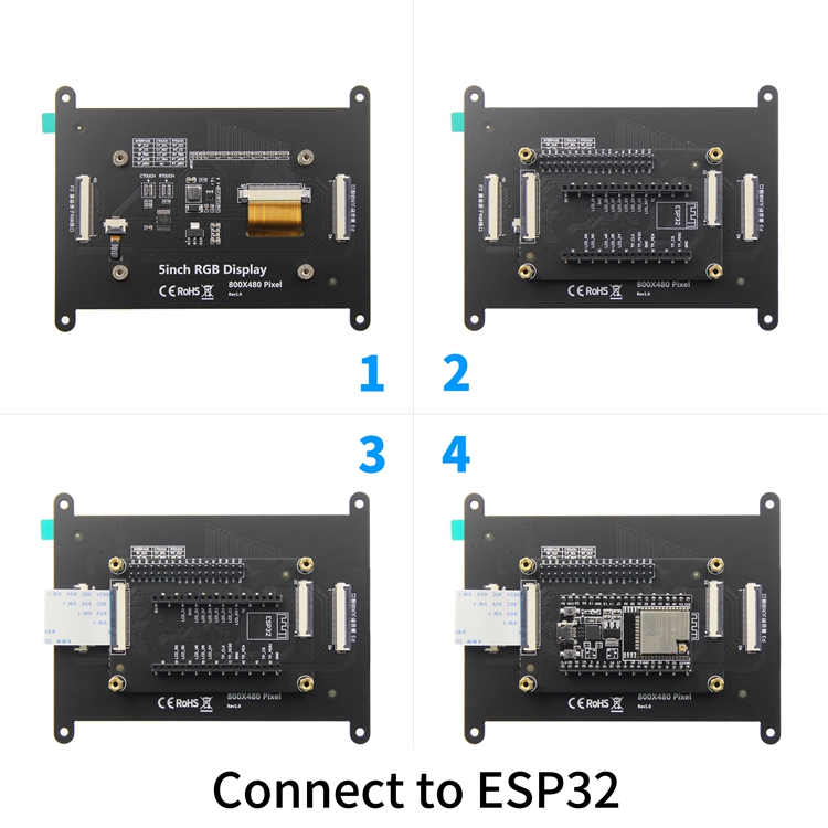
- Support direct insertion of esp32 development board
- Support direct connection of RGB display module flexible cable
- Support 8-bit and 16 bit parallel bus transmission, transmission speed block
- Provide rich STM32 platform and esp32 platform sample program
- Military grade process standard, long-term stable work
- Provide technical support for underlying driver
Product Parameters
| Name | Parameter |
| SKU | SSD1963 |
| Driver IC | SSD1963 |
| STM32 development board input interface | 16 bit parallel port |
| Input interface of esp32 development board | 8 bit parallel port |
| Output interface | 24 bit RGB parallel port |
| Module PCB Size | 50.00x77.00(mm) |
| Input Voltage | 5V |
| IO Voltage | 3.3V and 1.8V |
| Power Consumption | 36mA |
| Rough Weight(Net weight) | 22 (g) |
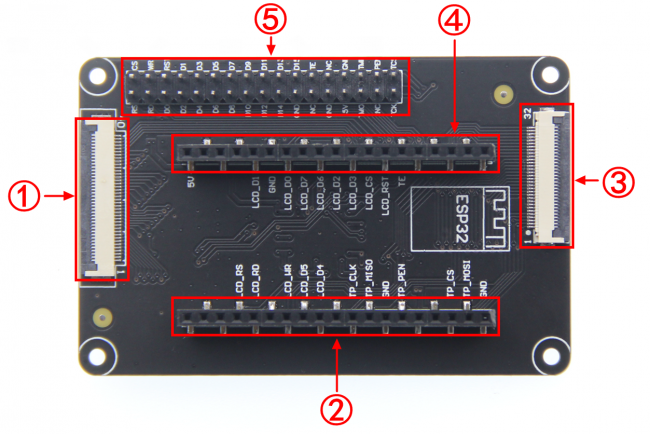
Interface Definition
- ①--40pin flexible cable output interface
- ②④--In line interface of esp32 development board
- ③--STM32 development board 32pin flexible cable input interface
- ⑤--STM32 development board 34pin pin input interface
- STM32 development board row pin input interface pin description
| Number | Pin name | Description |
| 1 | CS | LCD reset control pin( low level enable) |
| 2 | RS | LCD register / data selection control pin(high level: register, low level: data) |
| 3 | WR | LCD write control pin |
| 4 | RD | LCD read control pin |
| 5 | RST | LCD reset control pin( low level reset) |
| 6~21 | D0~D15 | LCD 16 bit data bus pin (use d0 ~ D7 in 8-bit mode) |
| 22 | GND | Module power ground pin |
| 23 | TE | LCD tearing effect signal pin (read only) |
| 24 | NC | No definition, reserved |
| 25 | NC | No definition, reserved |
| 26 | GND | Module power ground pin |
| 27 | GND | Module power ground pin |
| 28 | 5V | Module power supply positive pin (connected to 5V) |
| 29 | TMI | Resistance touch screen SPI bus read data pin (capacitor touch screen not used) |
| 30 | TMO | IIC bus data pin of capacitive touch screen (SPI bus write data pin of resistance touch screen) |
| 31 | PEN | Touch screen interrupt detection pin(Low level when a touch occurs) |
| 32 | NC | No definition, reserved |
| 33 | TCS | Capacitor touch screen reset pin (resistance touch screen chip selection pin) |
| 34 | TCK | IIC bus clock pin of capacitive touch screen (SPI bus clock pin of resistance touch screen) |
- STM32 development board flexible cable input interface pin description
| Number | Pin name | Description |
| 1 | TCK | IIC bus clock pin of capacitive touch screen (SPI bus clock pin of resistance touch screen) |
| 2 | TCS | Capacitor touch screen reset pin (resistance touch screen chip selection pin) |
| 3 | PEN | Touch screen interrupt detection pin(Low level when a touch occurs) |
| 4 | TMO | IIC bus data pin of capacitive touch screen (SPI bus write data pin of resistance touch screen) |
| 5 | TMI | Resistance touch screen SPI bus read data pin (capacitor touch screen not used) |
| 6 | 5V | Module power supply positive pin (connected to 5V) |
| 7 | GND | Module power ground pin |
| 8 | GND | Module power ground pin |
| 9 | NC | No definition, reserved |
| 10 | NC | No definition, reserved |
| 11 | TE | LCD tearing effect signal pin (read only) |
| 12~27 | D15~D0 | LCD 16 bit data bus pin (use d0 ~ D7 in 8-bit mode) |
| 28 | RST | LCD reset control pin( low level reset) |
| 29 | RD | LCD read control pin |
| 30 | WR | LCD write control pin |
| 31 | RS | LCD register / data selection control pin(high level: register, low level: data) |
| 32 | CS | LCD reset control pin( low level enable) |
- ESP32 development board in line interface pin description
| Number | Pin name | Description |
| 1 | 5V | power pin (connected to 5V) |
| 2 | LCD_RS | LCD register / data selection control pin(high level: register, low level: data) |
| 3 | LCD_RD | LCD read control pin |
| 4 | LCD_D1 | Pin 2 of 8-bit parallel data bus |
| 5 | GND | Power ground pin |
| 6 | LCD_WR | LCD write control pin |
| 7 | LCD_D0 | Pin 1 of 8-bit parallel data bus |
| 8 | LCD_D5 | Pin 6 of 8-bit parallel data bus |
| 9 | LCD_D7 | Pin 8 of 8-bit parallel data bus |
| 10 | LCD_D4 | Pin 5 of 8-bit parallel data bus |
| 11 | LCD_D6 | Pin 7 of 8-bit parallel data bus |
| 12 | LCD_D2 | Pin 3 of 8-bit parallel data bus |
| 13 | TP_CLK | IIC bus clock control pin of capacitive touch screen(SPI bus clock control pin of resistance touch screen) |
| 14 | LCD_D3 | Pin 4 of 8-bit parallel data bus |
| 15 | TP_MISO | SPI bus read data pin of resistance touch screen(capacitive touch screen not used) |
| 16 | LCD_CS | LCD chip select control pin |
| 17 | GND | Power ground pin |
| 18 | LCD_RST | LCD reset control pin |
| 19 | TP_PEN | Touch screen interrupt control pin |
| 20 | TE | Tearing Effect Signal pin(read-only) |
| 21 | TP_CS | Capacitive touch screen reset pin(resistance touch screen chip selection pin) |
| 22 | TP_MOSI | IIC bus data pin of capacitive touch screen(resistance touch screen SPI bus write data pin) |
| 23 | GND | Power ground pin |
- Pin description of flexible cable output interface
| Number | Pin name | Description |
| 1 | VCC5 | Power input pin(connect to 5V) |
| 2 | VCC5 | Power input pin(connect to 5V) |
| 3~10 | R0~R7 | 8-bit RED data pin |
| 11 | GND | power ground pin |
| 12~19 | G0 ~ G7 | 8-bit GREEN data pin |
| 20 | GND | power ground pin |
| 21~28 | B0 ~ B7 | 8-bit GREEN data pin |
| 29 | GND | power ground pin |
| 30 | PCLK | Pixel clock control pin |
| 31 | HSYNC | Horizontal synchronous signal control pin |
| 32 | VSYNC | Vertical synchronous signal control pin |
| 33 | DE | Data enable signal control pin |
| 34 | BL | LCD backlight control pin |
| 35 | TP_CS | Capacitor touch screen reset pin (resistance touch screen chip selection pin) |
| 36 | TP_MOSI | Data pin of IIC bus of capacitance touch screen (write data pin of SPI bus of resistance touch screen) |
| 37 | TP_MISO | Resistance touch screen SPI bus read data pin (capacitance touch screen not used) |
| 38 | TP_CLK | IIC bus clock control pin of capacitive touch screen (SPI bus clock control pin of resistance touch screen) |
| 39 | TP_PEN | Touch screen interrupt control pin (low level when touch is generated) |
| 40 | RST | LCD reset control pin (effective at low level) |

