More actions
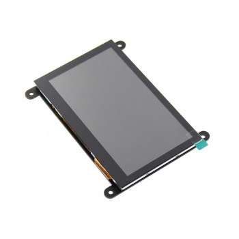
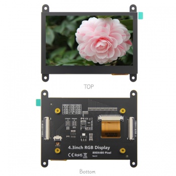
Product Picture
Product Description
- 4.3-inch color screen, support 24BIT RGB 16.7M color display, display rich colors
- Support 800x480, the display effect is very clear
- Support 24 bit RGB parallel bus transmission
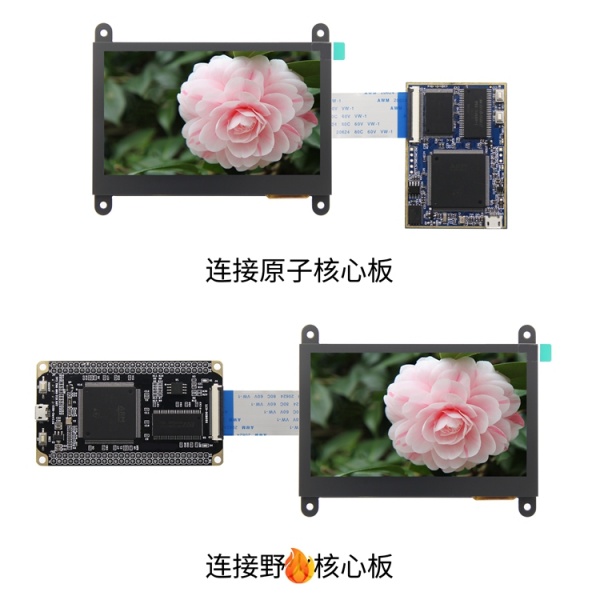
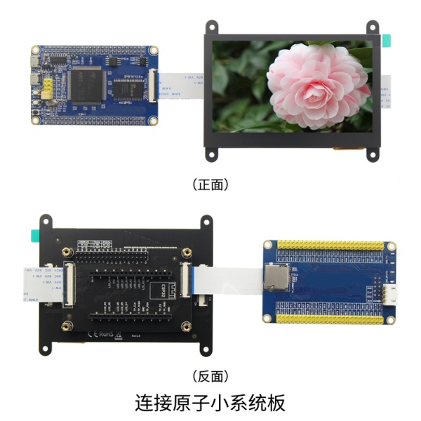
- Compatible with RGB interface connection of punctual atomic development board and wildfire development board
- It supports the switching between capacitive touch screen and resistance touch screen, and the capacitive touch screen can support up to 5 touch points
- Provides a rich sample program for STM32 platforms
- Military-grade process standards, long-term stable work
- Provide underlying driver technical support
Product Parameters
| Name | Parameter |
| Display Color | RGB888 16.7M (compatible with rgb5665k) color |
| SKU | MRG4301(no touch), MRG4311(have touch) |
| Screen Size | 4.3(inch) |
| Type | TFT |
| Driver IC | None |
| Resolution | 800*480 (Pixel) |
| Module Interface | 24Bit RGB parallel interface |
| Touch Screen Type | Capacitive or Resistive touch screen |
| Touch IC | FT5426(Capacitive touch), XPT2046(Resistive touch) |
| Active Area | 95.04x53.86(mm) |
| Module PCB Size | 105.41x86.41(mm) |
| Operating Temperature | -10℃~60℃ |
| Storage Temperature | -20℃~70℃ |
| Input Voltage | 5V |
| IO Voltage | 3.3V |
| Power Consumption | 50mA(The backlight is off), 165mA(The backlight is the brightest) |
| Rough Weight(Net weight) | 95(g) |
Interface Definition
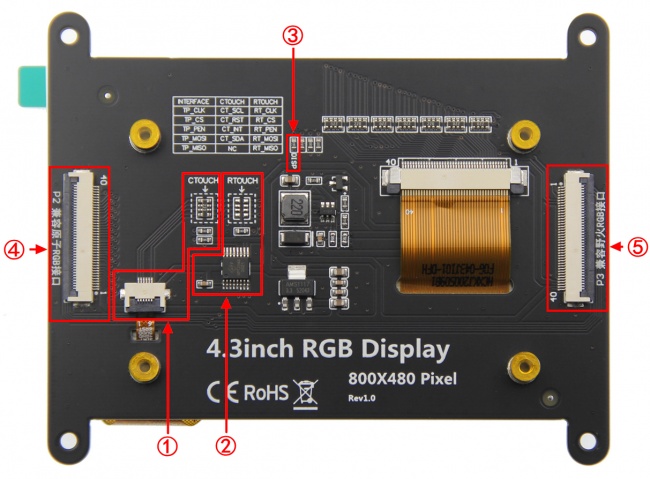
- ①--Capacitive touch screen circuit
- ②--Resistance touch screen circuit
- ③--Disp resistance
- ④--P2 interface (compatible with atomic RGB interface)
- ⑤--P3 interface (compatible with wildfire RGB interface)
1. Switch touch screen
- If you choose to connect the capacitive touch screen, please weld the capacitor touch screen circuit;
- Select the connection resistance touch screen, please weld the resistance touch screen circuit;
- If you often need to switch the touch screen, after welding other circuits, only switch the drain
- resistance in the dotted line box;
2. Precautions for disp resistance welding
- When connecting the wildfire development board for use, the disp resistance must be removed, otherwise
- the screen will not display after the development board is reset;
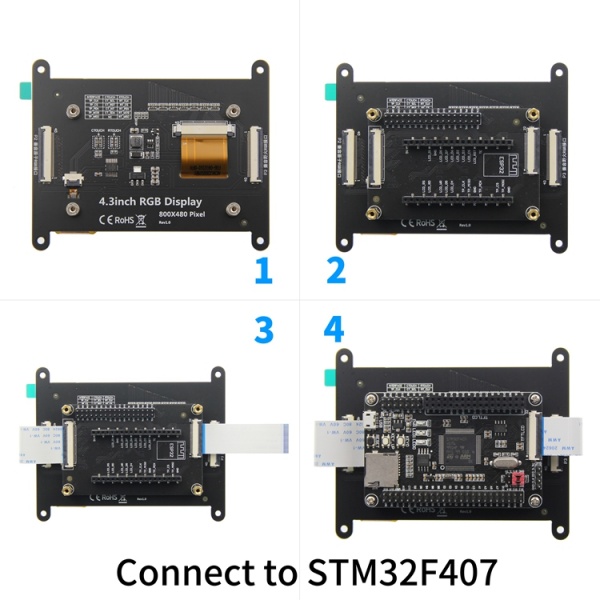
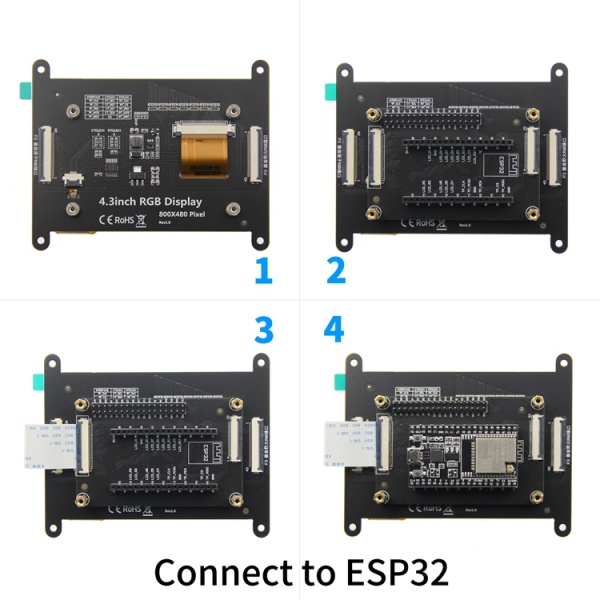
- When connecting atomic development board, f407 minimum system board or esp32 development board, disp
- resistance must be welded, otherwise the screen will not be displayed.
3. P2 and P3 interface pins are described as follows:
- P2 interface (compatible with atomic RGB interface) pin description
| Number | Pin name | Description |
| 1 | VCC5 | Power input pin(connect to 5V) |
| 2 | VCC5 | Power input pin(connect to 5V) |
| 3~10 | R0~R7 | 8-bit RED data pin |
| 11 | GND | power ground pin |
| 12~19 | G0 ~ G7 | 8-bit GREEN data pin |
| 20 | GND | power ground pin |
| 21~28 | B0 ~ B7 | 8-bit GREEN data pin |
| 29 | GND | power ground pin |
| 30 | PCLK | Pixel clock control pin |
| 31 | VSYNC | Vertical synchronous signal control pin |
| 32 | HSYNC | Horizontal synchronous signal control pin |
| 33 | DE | Data enable signal control pin |
| 34 | BL | LCD backlight control pin |
| 35 | TP_CS | Capacitor touch screen reset pin (resistance touch screen chip selection pin) |
| 36 | TP_MOSI | Data pin of IIC bus of capacitance touch screen (write data pin of SPI bus of resistance touch screen) |
| 37 | TP_MISO | Resistance touch screen SPI bus read data pin (capacitance touch screen not used) |
| 38 | TP_CLK | IIC bus clock control pin of capacitive touch screen (SPI bus clock control pin of resistance touch screen) |
| 39 | TP_PEN | Touch screen interrupt control pin (low level when touch is generated) |
| 40 | RST | LCD reset control pin (effective at low level) |
- P3 interface (compatible with wildfire RGB interface) pin description
| Number | Pin name | Description |
| 1 | TP_SCL | IIC bus clock control pin of capacitive touch screen |
| 2 | TP_SDA | Data pin of IIC bus of capacitance touch screen |
| 3 | TP_PEN | Touch screen interrupt control pin (low level when touch is generated) |
| 4 | TP_RST | Capacitor touch screen reset pin(enable at low level) |
| 5 | GND | power ground pin |
| 6 | BL | LCD backlight control pin |
| 7 | DISP | LCD display enable pin (enable at high level) |
| 8 | DE | Data enable signal control pin |
| 9 | HSYNC | Horizontal synchronous signal control pin |
| 10 | VSYNC | Vertical synchronous signal control pin |
| 11 | PCLK | Pixel clock control pin |
| 12~19 | B7 ~ B0 | 8-bit BLUE data pin |
| 20~27 | G7 ~ G0 | 8-bit GREEN data pin |
| 28~35 | R7 ~ R0 | 8-bit RED data pin |
| 36 | GND | power ground pin |
| 37 | VCC3.3 | Power input pin(connect to 3.3V) |
| 38 | VCC3.3 | Power input pin(connect to 3.3V) |
| 39 | VCC5 | Power input pin(connect to 5V) |
| 40 | VCC5 | Power input pin(connect to 5V) |
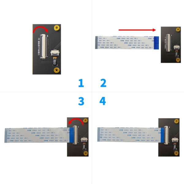
How to connect the development board
Program Download
Product Documentation
- 4.3inch RGB Display Module User Manual
- 4.3inch RGB TFTLCD Specification
- 4.3inch RGB Display Module Size Picture
- 4.3inch RGB Display Module Schematic
- 4.3inch RGB Display Module TFTLCD Schematic and PCB Package Library
- Capacitance touch IC FT5426 Data sheet
- Capacitance touch IC FT5426 Programming Guide
- Resistance touch screen control IC XPT2046 Data sheet
Reference Materials
- STM32 keil software use illustration
- PCtoLCD2002 software use illustration
- Image2Lcd software use illustration
- Chinese and English display modulo settings

