More actions
| Line 107: | Line 107: | ||
==<font color="blue">Product Documentation</font> == | ==<font color="blue">Product Documentation</font> == | ||
* [https://www.lcdwiki.com/res/ | * [https://www.lcdwiki.com/res/CH3202/CH32F103C8T6%E6%9C%80%E5%B0%8F%E7%B3%BB%E7%BB%9F%E6%9D%BF%E7%94%A8%E6%88%B7%E8%AF%B4%E6%98%8E.pdf '''CH32F103C8T6 Minimum system board user manual'''] | ||
* [https://www.lcdwiki.com/res/ | * [https://www.lcdwiki.com/res/CH3202/CH32F103C8T6%E6%9C%80%E5%B0%8F%E7%B3%BB%E7%BB%9F%E6%9D%BF%E5%B0%BA%E5%AF%B8%E5%9B%BE.pdf '''CH32F103C8T6 Minimum system board size drawing'''] | ||
* [https://www.lcdwiki.com/res/ | * [https://www.lcdwiki.com/res/CH3202/CH32F103C8T6%E6%9C%80%E5%B0%8F%E7%B3%BB%E7%BB%9F%E6%9D%BF%E5%8E%9F%E7%90%86%E5%9B%BE.pdf '''CH32F103C8T6 minimum system board Schematic diagram'''] | ||
* [https://www.lcdwiki.com/res/ | * [https://www.lcdwiki.com/res/CH3202/CH32F103C8T6%E6%9C%80%E5%B0%8F%E7%B3%BB%E7%BB%9F%E6%9D%BFIO%E8%B5%84%E6%BA%90%E5%88%86%E9%85%8D%E8%A1%A8.xlsx '''CH32F103C8T6 Minimum system board IO resource allocation table'''] | ||
* [https://www.lcdwiki.com/res/ | * [https://www.lcdwiki.com/res/CH3202/SCHLIB.zip '''CH32F103C8T6 Minimum system board schematic Library'''] | ||
* [https://www.lcdwiki.com/res/ | * [https://www.lcdwiki.com/res/CH3202/PCBLIB.zip '''CH32F103C8T6 Minimum system board PCB package library'''] | ||
* [https://www.lcdwiki.com/res/ | * [https://www.lcdwiki.com/res/CH3202/CH32F103DS0.PDF '''CH32F103C8T6 Data Sheet'''] | ||
* [https://www.lcdwiki.com/res/CH3202/CH32F103DS1.PDF '''CH32F103C8T6 Quick application manual'''] | |||
* [https://www.lcdwiki.com/res/CH3202/CH32xRM.PDF '''CH32X Series application manual'''] | |||
==<font color="blue">Reference Materials</font> == | ==<font color="blue">Reference Materials</font> == | ||
Revision as of 16:21, 3 September 2021
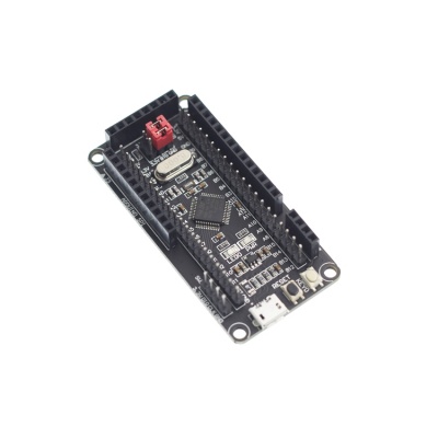
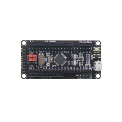
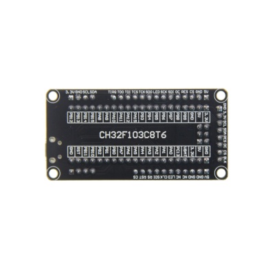
CH32F103C8T6 Minimum System Development Board
Product Picture
Product Description
- CPU: CH32F103C8T6, main frequency: 72MHz, internal FLASH: 64KB, internal SRAM: 20KB
- Small and delicate appearance, convenient for various DIY projects
- Support SWD and serial download, easy to debug
- Support SPI interface and IIC interface display module direct insertion
- Extended GPIO port for easy connection to various peripherals
- Rich development resources, easy to learn, easy to get started
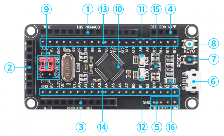
Product Parameters
| Serial number | Name | Description |
| ① | J1 | Connect to the Common-SPI display module |
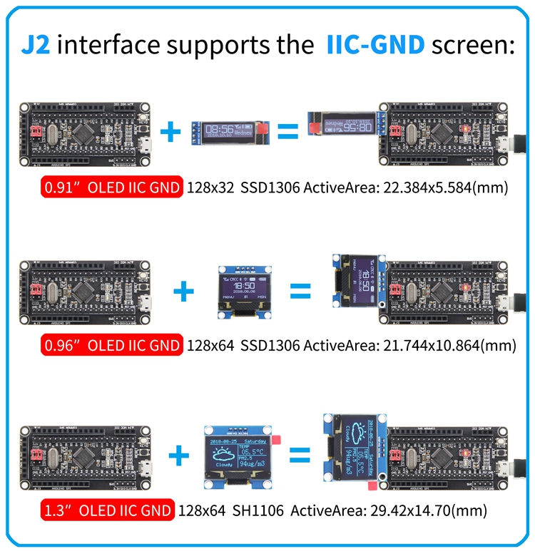
| ② | J2 | Connect to the Common-SPI/IPS display module |
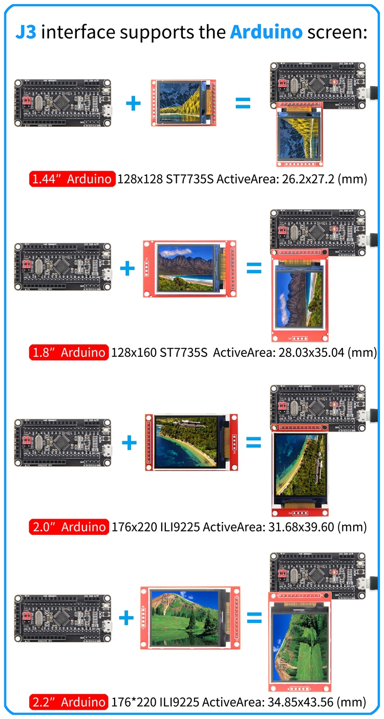
| ③ | J3 | Connect to the Arduino-SPI display module |
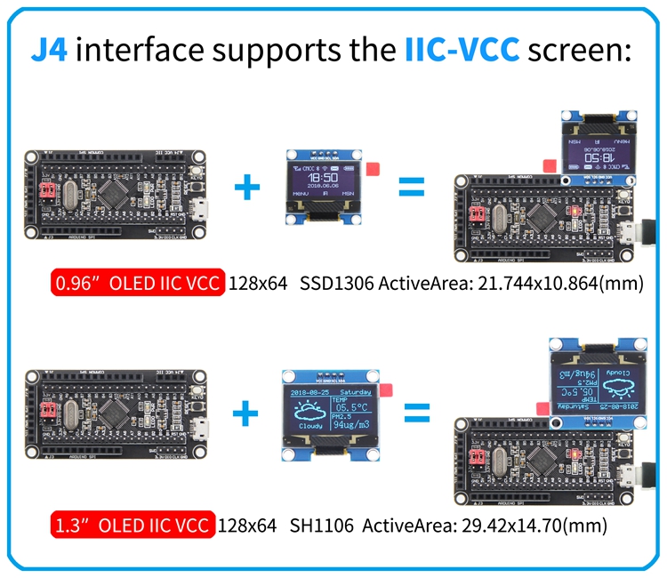
| ④ | J4 | Connect to the IIC-VCC display module |
| ⑤ | SWD | For SWD download and emulation |
| ⑥ | USB interface | Used for USB communication and power supply |
| ⑦ | Reset button | Reset development board |
| ⑧ | KEY0 | For standby wake up or program button function design |
| ⑨ | BT0/BT1 | Used to select the startup mode after the development board is reset |
| ⑩ | STM32F103C8T6 | Main chip, main frequency: 72MHz, internal FLASH: 64KB, internal SRAM: 20KB, support RTC, interrupt, PWM, DMA and other functions |
| ⑪ | Power light | Red LED light is used to indicate whether the development board is normally powered |
| ⑫ | LED0 | Blue LED light, used to indicate the running status of the program and DIY program lighting effect design |
| ⑬,⑭ | IO expand | It is used to connect various peripherals to facilitate project development |
| ⑮ | Power stabilized IC | 5V in,3.3V out |
| ⑯ | Self restoring fuse | Ensure the safety of the circuit in case of short circuit or other fault |
How to connect LCD screen
Program Download
Product Documentation
- CH32F103C8T6 Minimum system board user manual
- CH32F103C8T6 Minimum system board size drawing
- CH32F103C8T6 minimum system board Schematic diagram
- CH32F103C8T6 Minimum system board IO resource allocation table
- CH32F103C8T6 Minimum system board schematic Library
- CH32F103C8T6 Minimum system board PCB package library
- CH32F103C8T6 Data Sheet
- CH32F103C8T6 Quick application manual
- CH32X Series application manual

