More actions
| (4 intermediate revisions by the same user not shown) | |||
| Line 17: | Line 17: | ||
| style="width: 80px" align="center" |PIN | | style="width: 80px" align="center" |PIN | ||
| align="center" |D1 miniDevelopment board corresponding wiring pin | | align="center" |D1 miniDevelopment board corresponding wiring pin | ||
| align="center" | | | align="center" |Pin Description | ||
|- | |- | ||
| align="center" |1 | | align="center" |1 | ||
| Line 67: | Line 67: | ||
== <font color="blue">Program Download</font> == | == <font color="blue">Program Download</font> == | ||
* [https://www.lcdwiki.com/res/ | * [https://www.lcdwiki.com/res/MSP1443/Simple_Module_ESP8266_Demo.zip '''1.44inch module test program'''] | ||
==<font color="blue">Using Description</font> == | ==<font color="blue">Using Description</font> == | ||
* [https://www.lcdwiki.com/res/ | * [https://www.lcdwiki.com/res/MSP1443/1.44inch_SPI_Simple_Module_User_Manual_EN.pdf '''1.44inch module ESP8266 User Manual'''] | ||
* [https://www.lcdwiki.com/res/PublicFile/Arduino_IDE_Use_Illustration_EN.pdf '''Arduino IDE software use illustration'''] | |||
Latest revision as of 16:52, 19 January 2021
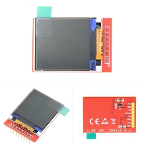
Product Picture
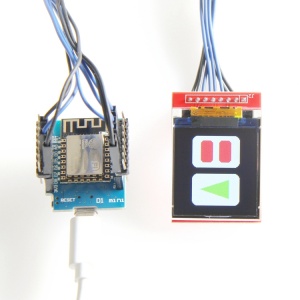
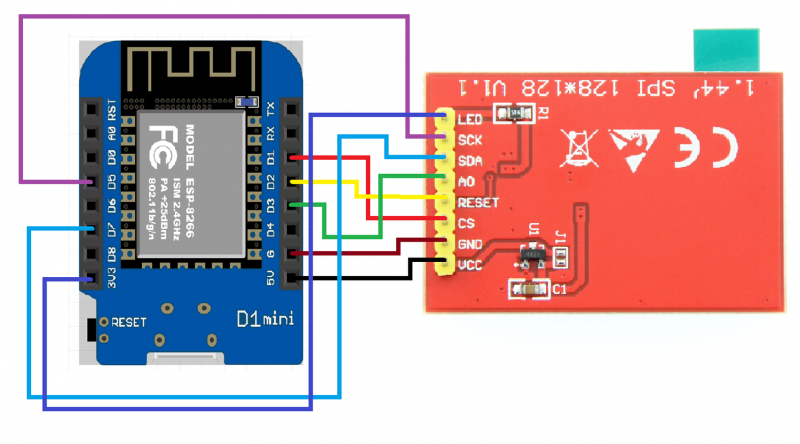
Wiring Description
| NUMBER | PIN | D1 miniDevelopment board corresponding wiring pin | Pin Description |
| 1 | LED | 3.3V | LCD backlight control pin( connect to 3.3V) |
| 2 | SCK | D5 | LCD SPI bus clock pin |
| 3 | SDA | D7 | LCD SPI bus write data pin |
| 4 | A0/DC | D3 | LCD register / data selection control pin |
| 5 | RESET | D2 | LCD reset control pin |
| 6 | CS | D1 | LCD chip selection control pin |
| 7 | GND | G | Power ground |
| 8 | VCC | 5V | Power positive |

